Laser melting systems are increasingly being used in high-value sectors like aerospace and automotive to manufacture metallic and plastics parts in layers from powder.
However, this process reportedly comes with its limitations as it relies on a mirror to deflect a single laser, curbing the speed of the system.
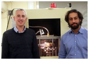
A new process developed at the University of Sheffield in the United Kingdom, called diode area melting (DAM), can overcome this by melting large areas in parallel using an array of individual laser diodes.
These laser beams can be switched on or off as they move across the powder bed making it faster but also more energy efficient.
Dr. Kristian Groom, from the Department of Electronic and Electrical Engineering, said: “Our research challenges the long-held belief in the industry that low power diode modules cannot achieve sufficient melting due to their low power and poor beam quality”.
“Key to the success of the DAM process was a move to shorter wavelength laser arrays (of 808 nm) where increased absorption of the individually collimated and focused beams allowed melting points in excess of 1400℃ to be reached within a few milliseconds, enabling production of fully dense stainless steel 17-4 parts.”
Inventors of the DAM process Groom and Dr. Kamran Mumtaz (Department of Mechanical Engineering) plan to continue the research investigating laser interaction whilst broader plans are for scaling-up the system and extending to polymer processing.
The team believe it may be possible to combine wavelength-targeted processing of a wide range of materials in one machine.
The research has been supported by proof of concept funding from an Engineering and Physical Sciences Research Council (EPSRC) allocated impact acceleration grant (IIKE).


